



































































































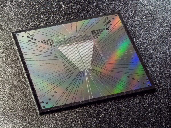
For nearly five years, 26 research institutions, companies and start-ups have joined forces in QSolid to develop a quantum computer using cutting-edge German technology: a 30-qubit quantum chip with low error rates. With several competitive demonstrators, the project has more than achieved this goal. In addition to a 10-qubit system that has already been tested and made accessible to users, the consortium is currently testing a 30-qubit system, with promising results. Using demonstration applications, such as the modelling of spin resonance processes employed in chemical analysis and magnetic resonance imaging (MRI), the interaction between hardware and software could be investigated under realistic conditions. One of the project’s technological achievements is the development of a particularly fast quantum gate that sets new international benchmarks for switching speed. Quantum gates play a crucial role in quantum computers: they perform computational operations that can change the state of a qubit, thereby forming the basis for information processing in a quantum computer. “The performance of a quantum computer depends on how many computational steps it can carry out while keeping errors to a minimum. There are two main ways to achieve this: we can either ensure that qubits retain their quantum states for longer or speed up gate operations, allowing more computational steps to be performed in the same amount of time,” explains Prof. Frank Wilhelm-Mauch of Forschungszentrum Jülich, who coordinates the large-scale project. “In QSolid, we have made important methodological advances, particularly in gate speed, that extend far beyond the project itself. They demonstrate that we have highly capable components and that the integration of hardware and software has already reached a high level of maturity,” says the quantum physicist and Director of the Peter Grünberg Institute for Quantum Computing Analytics (PGI-12). Fraunhofer IPMS: Established semiconductor technology supports the scalable manufacturing of quantum processors Fraunhofer IPMS has made significant contributions to the development of scalable quantum processors through QSolid. The focus was on the cryogenic characterization of CMOS circuits in collaboration with GlobalFoundries, ADMOS, and RacyICs. In addition, an innovative advanced packaging solution was developed jointly with Fraunhofer IZM-ASSID as part of the Center for Advanced CMOS and Heterointegration Saxony (CEASAX). So-called interposers are used to connect the quantum chip and the control chip in a space-saving manner. The key challenge is to reliably transmit signals while simultaneously protecting the sensitive quantum chips from heat. The work builds on proven processes from industrial silicon semiconductor manufacturing and contributes to the future realization of quantum processors with significantly more qubits. Dr. Benjamin Lilienthal-Uhlig of Fraunhofer IPMS explains: “Through our work on the QSolid project, we have demonstrated how proven technologies from industrial semiconductor manufacturing can be leveraged for the development of future quantum computers. The combination of cryogenic control electronics and innovative interconnection technologies is an important step toward making quantum processors more powerful and more scalable in the future.” Collaboration Between Research and Industry One of QSolid’s key achievements has been to bring together expertise previously distributed across numerous locations and partners and channel it into the joint development of a large-scale scientific instrument. “With QSolid, we have demonstrated that here in Germany we can design, manufacture and operate functional quantum processors from scratch within a short period of time. This is a crucial prerequisite for the further development of the German quantum ecosystem and a major achievement for the highly skilled students, scientists and engineers who made it possible,” explains Prof. Rami Barends, Director of the Peter Grünberg Institute for Functional Quantum Systems (PGI-13) at Forschungszentrum Jülich, which was established shortly before the project began. A professional, collaborative systems engineering approach, building on methods originally developed for the space sector, enabled specialised partners to test their technologies together and successfully combine and further develop them into integrated quantum systems. Alongside Forschungszentrum Jülich, the Leibniz Institute of Photonic Technology (Leibniz-IPHT) in Jena, the CiS Forschungsinstitut für Mikrosensorik in Erfurt, the Karlsruhe Institute of Technology (KIT) and the Physikalisch-Technische Bundesanstalt (PTB) in Braunschweig contributed their expertise. The software also reflects the close collaboration within the consortium. The software stack of the current demonstrators combines solutions from Zurich Instruments, Qruise, Bull, ParityQC and HQS Quantum Simulations. Innovative hardware components, such as connectors from Rosenberger and cables from Supracon, have also made a significant contribution to improving the performance of the quantum computers. Successful closing of the project From 27 to 29 October, project participants from different parts of Germany will gather in Jülich for the project’s closing event to present their results and discuss insights gained from their collaborative work. The achievements range from tested quantum computer prototypes accessible via the cloud to expertise that has already been translated into concrete products and services. The project, which received 76.3 million euros in funding from the Federal Ministry of Research, Technology, and Space (grant number 13N16150) has pooled expertise from across Germany and brought together partners from research and industry. By jointly developing a quantum ecosystem, the consortium has given companies early access to this emerging technology and strengthened their technological capabilities and independence. Photo credit: 30-qubit chip, ©Forschungszentrum Jülich / PGI-13
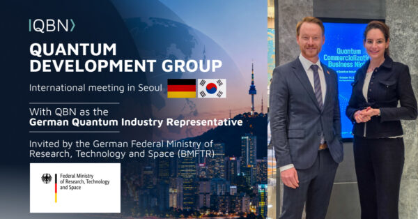
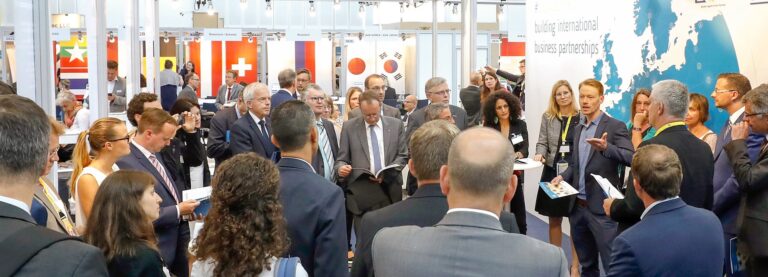
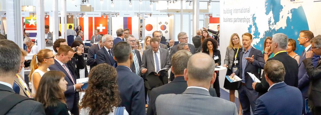
SEOUL, REPUBLIC OF KOREA / MUNICH, GERMANY – On invitation from the German Federal Ministry of Research, Technology and Space (BMFTR), Johannes Verst, CEO of Quantum Business Network (QBN), joined the German delegation at the Quantum Development Group (QDG) meeting in Seoul to represent the German quantum industry during the dedicated industry session. The QDG is a multilateral initiative of 13 countries – bringing together the Republic of Korea, the United States, Britain, France, Germany, Japan, Australia, Denmark, Finland, Canada, Sweden, the Netherlands and Switzerland – promoting international cooperation on the responsible development and commercialisation of quantum technologies. Following the ministry-level sessions, QBN engaged in bilateral exchanges with international delegations as well as attendees at the subsequent Quantum Technology Business Forum. Orchestrating Technology Push and Market Pull While Germany and its global partners boast world-class research infrastructure and strong government backing, scaling deep-tech capabilities requires an active demand side. During discussions around commercial deployment and ecosystem cooperation, QBN highlighted the need to move beyond technical potential toward concrete business cases that deliver clear economic return for adoption partners. “Germany’s industrial foundation in quantum, key enabling technologies and corporate end-users is exceptionally strong,” said Johannes Verst, CEO of QBN. “However, sustainable scaling will not happen through tech push alone. We must establish structured market demand across core sectors such as automotive, aerospace, chemical and defence. To achieve this, public policy must combine targeted funding for existing industrial strengths with clear economic and security objectives. We are deeply appreciative of the BMFTR’s continued trust and invitation to represent the German quantum ecosystem on this key multilateral platform. “ Furthermore, QBN emphasized that capital follows transparent demand markets. Unclear adoption pathways and fragmented export controls often deter private capital. By helping public and corporate buyers build structured procurement roadmaps, QBN enables high-tech suppliers to validate commercial demand and secure growth capital. Countering Ecosystem Fragmentation Through Global Alliances A central theme of QBN’s contributions in Seoul was the necessity of avoiding organisational and national fragmentation. Building redundant local capabilities or isolated national silos dilutes resources and slows down commercial progress. True technological sovereignty for Germany and Europe relies on access to distributed, trusted and interoperable allied supply chains across Europe, North America and Asia-Pacific. QBN operates as an agile, overarching platform designed to connect regional industrial hubs directly to international markets and multilateral policy initiatives. By providing a trusted B2B platform, QBN enables high-tech SMEs, industrial scale-ups and corporate end-users to secure cross-border supply chains, access growth capital and drive real-world adoption. About QBN QBN is the global quantum alliance and B2B platform dedicated to advancing the quantum industry. Deeply rooted in Europe’s industrial core, QBN connects science, industry, investment and policy to accelerate commercialisation, industry adoption and scaling of quantum technologies. Media Contact: Email: info@qbn.world Website: www.qbn.world
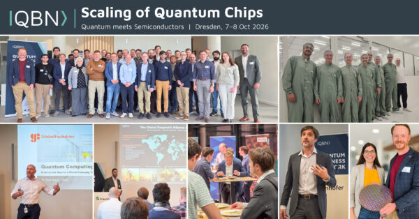
Quantum meets Semiconductors QBN brought quantum hardware developers, semiconductor specialists, equipment suppliers, researchers and policymakers together at Fraunhofer IPMS in Dresden on 7–8 October 2026. The Scaling of Quantum Chips workshop connected technical bottlenecks with the industrial conditions needed to overcome them. A recurring finding was that progress in individual devices must be matched by progress in manufacturing, testing, infrastructure and commercial deployment. Scaling plans must cover the entire quantum computing system. Hardware and algorithm teams need to align their requirements through co-design. Packaging, control electronics and, where required, cryogenics must influence processor design and fabrication from the outset. These dependencies require developers to involve suppliers early. A processor that becomes more demanding to connect, cool or test can shift the scaling bottleneck into another part of the system. The manufacturing goal must be consistent performance across larger numbers of processors and systems. A single “hero device” cannot demonstrate that. Developers and manufacturers must assess performance variation and the share of devices meeting requirements. Characterisation results must feed back into fabrication and system design, so the process improves the consistency of subsequent devices. Testing must develop into a repeatable industrial process. Automated characterisation requires integrated measurement workflows. Hardware teams, test providers and, where needed, cryogenics specialists must coordinate equipment, measurement sequences and operating conditions. Test throughput must match planned production volumes. For cryogenic systems, cooling must support rapid measurement cycles during development and be expandable as operational systems grow. The semiconductor industry is an important partner in addressing these challenges. Both communities must identify which established manufacturing and testing methods suit quantum requirements and where adaptation is necessary. Business leaders and engineers must work from the same assumptions about performance, cost and realistic production volumes. Manufacturing and business models must reflect these conditions; conventional semiconductor economies of scale cannot simply be assumed for quantum hardware. Europe needs financing and infrastructure access that support the transition to industrial production. Funding bodies and investors must address the capital required between development and deployment. Infrastructure providers must establish practical access to the fabrication, design and testing capabilities companies need. Research organisations, suppliers and facility operators must coordinate existing strengths around concrete industrial requirements. Customer demand must guide that development. Suppliers and industrial users need to define the performance, reliability and operating conditions an application requires, and assess usability and cost against the intended customer’s needs. A technically capable system must address a defined customer problem and be practical to operate. QBN will continue this work through its Working Group Quantum Computing & Applications. Get in touch with QBN to explore quantum opportunities for your business and connect with the right expertise and partners.
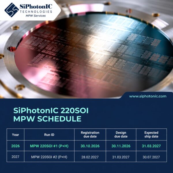
Copenhagen, 8 October 2026. SiPhotonIC, a Danish photonic foundry providing fast and flexible photonic integrated circuit fabrication and prototyping across SOI, SiN, TFLN and custom photonic platforms, announces the launch of its SOI Multi-Project Wafer (MPW) service pipeline, providing researchers and companies with accessible and cost-effective access to silicon photonics fabrication. The new MPW service enables multiple participants to share a wafer fabrication run, significantly reducing the cost and entry barrier associated with photonic integrated circuit development. Based on SiPhotonIC’s 220 nm SOI platform, the service combines established fabrication processes with dedicated PDKs and flexible design options, enabling rapid prototyping of passive silicon photonic circuits with integrated thermo-optic heaters. Launching the first 220SOI MPW run The first SiPhotonIC 220SOI MPW run (MPW #1) is now open for registration. The platform is optimized for C-band silicon photonics and supports passive photonic circuits with integrated thermo-optic heaters. MPW #1 schedule: Registration deadline: 30 October 2026 GDS submission deadline: 30 November 2026 Expected shipment: 31 March 2027 The MPW offering provides flexible design areas of 5 × 5 mm, 5 × 10 mm and 10 × 10 mm, allowing participants to select an appropriate footprint for their PIC designs while sharing the cost of wafer fabrication with other users. Standard delivery includes packs of 12 PICs, with additional packs of +12 PICs available as an option. The service is aimed at both academic and industrial users developing photonic integrated circuits for applications including optical communications, sensing, quantum photonics and other emerging photonic technologies. Discounts are available for academic users. From MPW prototyping to custom fabrication The MPW service complements SiPhotonIC’s existing on-demand prototyping model, providing dedicated fabrication for projects where speed and process flexibility are more important than the cost advantages of a shared wafer run. SiPhotonIC also offers custom nanofabrication pipelines for projects requiring specialized process flows, materials, device geometries or fabrication steps. This provides customers with a path from initial concept and prototyping to increasingly customized photonic fabrication requirements. Together, these access modes allow customers to choose between cost-optimized MPW fabrication, fast dedicated prototyping and fully customized process development, depending on their technical and scheduling requirements. Expanding the SiPhotonIC MPW service Following the first 220SOI MPW, SiPhotonIC plans to launch another 220SOI MPW run in early 2027. The company is also working toward expanding its MPW offering with O-band compatibility and active photonic devices, including modulators and photodiodes, further broadening the range of applications supported by the SOI platform. Access modes to SiPhotonIC services and technologies SiPhotonIC provides several flexible access routes to its fabrication technologies: On-demand prototyping runs — Fast, dedicated fabrication for individual designs, with typical delivery times of 1–3 months. Multi-Project Wafer (MPW) runs — Shared wafer fabrication providing an optimized cost structure on a fixed schedule. Custom stack development — Dedicated development of novel photonic stacks, materials and fabrication processes. Early access to new fabrication technologies — Discounted access schemes for customers participating in or co-developing new technologies. Photonic platforms Silicon-on-Insulator (SOI): 220SOI, 250SOI and custom SOI Silicon Nitride (SiN): 300SiN, 100–800 nm SiN and custom SiN Thin-Film Lithium Niobate (TFLN): 400TFLN SiN-on-SOI: Custom platforms and process stacks Relevant photonic cleanroom processes (deposition, etching, metrology etc.): on demand Contact For business enquiries, fabrication orders or MPW registration: info@siphotonic.com www.siphotonic.com About SiPhotonIC SiPhotonIC is a Danish photonic foundry providing fast, flexible and cost-effective photonic integrated circuit prototyping and fabrication services. Operating through DTU Nanolab and a network of partners, SiPhotonIC supports a broad range of photonic platforms, including SOI, SiN and TFLN, with access modes ranging from on-demand prototyping and MPW runs to custom process development and early access to new technologies.