The Fraunhofer Institute for Photonic Microsystems IPMS is one of the leading organisations for research, development and the pilot manufacturing of Photonic Microsystems.
CENTER NANOELECTRONIC TECHNOLOGIES (CNT)
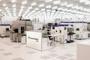 The Center Nanoelectronic Technologies (CNT), a division, within Fraunhofer IPMS, conducts research on 300 mm wafers for microchip producers, suppliers, equipment manufacturers and R&D partners and offers technology development and services on Ultra Large Scale Integration Level (ULSI) in the area of FEoL and BEoL. CNT develops semiconductor technologies on 300 mm wafers and work on the integration of innovative functionalities into existing CMOS platforms. One focus is currently on research into novel memory concepts and high-frequency components based on ferroelectric, CMOS-compatible materials. Furthermore, the CNT is working on energy-efficient power management systems that combine solid state batteries, harvesters and embedded capacitors. Moreover, neuromorphic systems and components with e.g. spin-based devices as well as technologies towards quantum computing are investigated.
For its research, CNT uses a flexibly usable tool park and a wide range of processes. The existing screening-fab concept enables consumables suppliers, equipment manufacturers and semiconductor companies to test new materials and manufacturing processes. The services offered range from the qualification of manufacturing steps such as cleaning or etching, copper plating and CMP to the evaluation of new precursors for atomic layer deposition. In addition, CNT supplies a wide range of methods for physical failure analysis and wafer level electrical characterization of semiconductor devices.
Applications:
•Qubit technologies for the use of semiconductor manufacturing
•Interface to classic CMOS electronics
•Focus on large technology and industrial compatibility
DATA COMMUNICATION AND COMPUTING (DCC)
 The Data Communication and Computing (DCC) division at Fraunhofer IPMS specializes in advanced communication technologies and computing systems. It focuses on developing innovative solutions in areas such as IP-Cores, optical wireless communication, and quantum technologies. The DCC team employs cutting-edge research to create high-performance solutions that enable efficient, reliable, and safe data transfer across various industries, including telecommunications, automotive, and industrial automation.
The DCC team is expert in various cutting-edge quantum technologies. This includes quantum key distribution (QKD) to ensure secure communication channels and the development of quantum random number generators (QRNG) that leverage fundamental quantum phenomena for robust security. By integrating these advanced technologies, the DCC department positions itself at the forefront of communication solutions, addressing the evolving needs for security and efficiency in data transfer.
