Telecom single-photon detector characterization

Semi-automatic cryogenic wafer prober for I-V characterisation of III-V photodetectors, especially InGaAs/InP pin-PDs, APDs, and SPADs. Wafer diameters: 76.2 mm (3 inch), 100 mm (4 inch); multi-project wafer compatibility; cryogenic cooling option, temperature range: 77 – 300 K. Laborarory setup for electrooptical characterisation of III-V photodetectors on chip level, especially InGaAs/InP pin-PDs, APDs, and SPADs, with respect to dark-current / dark-count characteristics, spectral responsivity, photon-detection efficiency, afterpulsing etc.; chip size < 10 x 10 mm²; pulsed laser wavelength: 1550 nm; cryogenic cooling option, temperature range: 77 – 300 K.
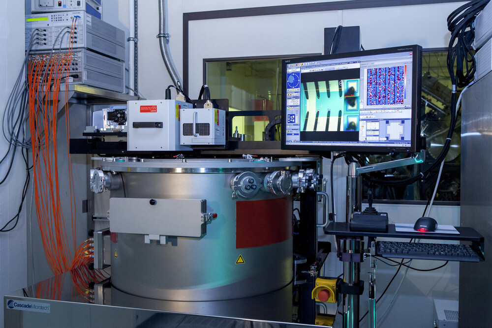
Telecom single-photon detector characterization

Key Insights & References

Value proposition

III-V quantum photodetector characterisation service, wafer and chip level, cryogenic cooling option

Bottleneck of SOTA

Wafer-level characterisation is important for short feedback loops during the development and fabrication of III-V photodetectors. The option for cryogenic cooling of the wafer or chip samples during electrooptical characterisation of the photodetector key parameters is rarely available.

Year Published

2025

Application Area

General

Quantum Sensing & Imaging

Sensing/Imaging Type

Photon Detection

Device Type

Quantum Photodetectors

Operating Environment

77 - 300 K

Performance Metrics

Dynamic Range

10 mA - 10 fA dark / photo current

Sensitivity

single photons, typ. PDE ~ 25%

Resolution

> 50 ps

Quantum Business Network

We Build a Strong Quantum Industry Together!

Login in on QBN Platform

Issues logging in?

or