

Copenhagen, 8 October 2026. SiPhotonIC, a Danish photonic foundry providing fast and flexible photonic integrated circuit fabrication and prototyping across SOI, SiN, TFLN and custom photonic platforms, announces the launch of its SOI Multi-Project Wafer (MPW) service pipeline, providing researchers and companies with accessible and cost-effective access to silicon photonics fabrication.
The new MPW service enables multiple participants to share a wafer fabrication run, significantly reducing the cost and entry barrier associated with photonic integrated circuit development. Based on SiPhotonIC’s 220 nm SOI platform, the service combines established fabrication processes with dedicated PDKs and flexible design options, enabling rapid prototyping of passive silicon photonic circuits with integrated thermo-optic heaters.
Launching the first 220SOI MPW run
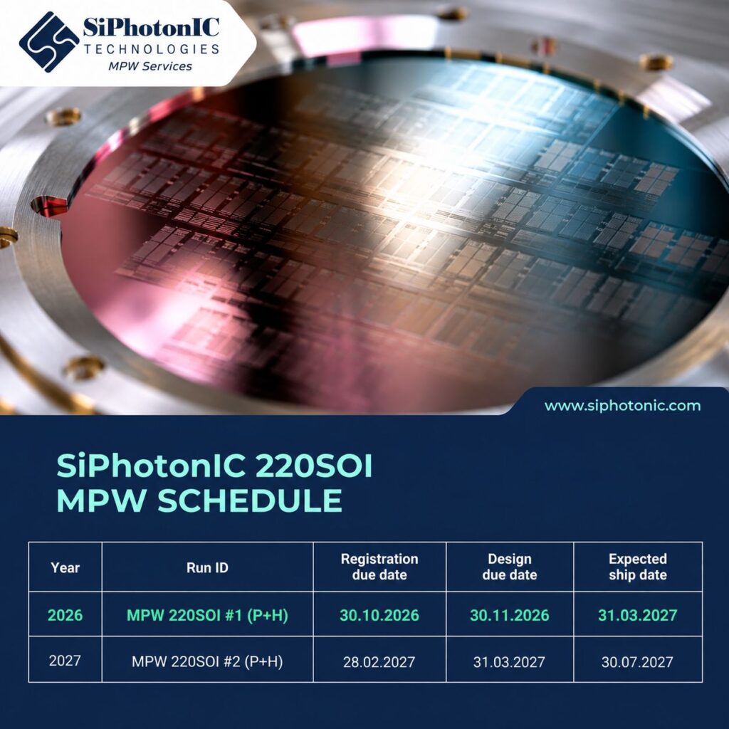
The first SiPhotonIC 220SOI MPW run (MPW #1) is now open for registration. The platform is optimized for C-band silicon photonics and supports passive photonic circuits with integrated thermo-optic heaters.
MPW #1 schedule:
Registration deadline: 30 October 2026
GDS submission deadline: 30 November 2026
Expected shipment: 31 March 2027
The MPW offering provides flexible design areas of 5 × 5 mm, 5 × 10 mm and 10 × 10 mm, allowing participants to select an appropriate footprint for their PIC designs while sharing the cost of wafer fabrication with other users. Standard delivery includes packs of 12 PICs, with additional packs of +12 PICs available as an option.
The service is aimed at both academic and industrial users developing photonic integrated circuits for applications including optical communications, sensing, quantum photonics and other emerging photonic technologies. Discounts are available for academic users.
From MPW prototyping to custom fabrication
The MPW service complements SiPhotonIC’s existing on-demand prototyping model, providing dedicated fabrication for projects where speed and process flexibility are more important than the cost advantages of a shared wafer run.
SiPhotonIC also offers custom nanofabrication pipelines for projects requiring specialized process flows, materials, device geometries or fabrication steps. This provides customers with a path from initial concept and prototyping to increasingly customized photonic fabrication requirements.
Together, these access modes allow customers to choose between cost-optimized MPW fabrication, fast dedicated prototyping and fully customized process development, depending on their technical and scheduling requirements.
Expanding the SiPhotonIC MPW service
Following the first 220SOI MPW, SiPhotonIC plans to launch another 220SOI MPW run in early 2027. The company is also working toward expanding its MPW offering with O-band compatibility and active photonic devices, including modulators and photodiodes, further broadening the range of applications supported by the SOI platform.
Access modes to SiPhotonIC services and technologies
SiPhotonIC provides several flexible access routes to its fabrication technologies:
- On-demand prototyping runs — Fast, dedicated fabrication for individual designs, with typical delivery times of 1–3 months.
- Multi-Project Wafer (MPW) runs — Shared wafer fabrication providing an optimized cost structure on a fixed schedule.
- Custom stack development — Dedicated development of novel photonic stacks, materials and fabrication processes.
- Early access to new fabrication technologies — Discounted access schemes for customers participating in or co-developing new technologies.
Photonic platforms
- Silicon-on-Insulator (SOI): 220SOI, 250SOI and custom SOI
- Silicon Nitride (SiN): 300SiN, 100–800 nm SiN and custom SiN
- Thin-Film Lithium Niobate (TFLN): 400TFLN
- SiN-on-SOI: Custom platforms and process stacks
- Relevant photonic cleanroom processes (deposition, etching, metrology etc.): on demand
Contact
For business enquiries, fabrication orders or MPW registration: info@siphotonic.com
About SiPhotonIC
SiPhotonIC is a Danish photonic foundry providing fast, flexible and cost-effective photonic integrated circuit prototyping and fabrication services. Operating through DTU Nanolab and a network of partners, SiPhotonIC supports a broad range of photonic platforms, including SOI, SiN and TFLN, with access modes ranging from on-demand prototyping and MPW runs to custom process development and early access to new technologies.
